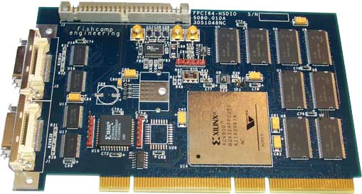
This card was used in a video image frame grabber application. It included an LVDS interface for the connection to an external camera and 128 MBytes of on-board SDRAM for image storage. Much of the logic, including the PCI interface, was implemented inside a Xilinx FPGA chip. This allowed the card to be changed if needed to accommodate different camera interface specs.
The main clock generator was implemented with DDS technology in order to be able to synthesize a wide range of master clocks for the camera interface timing.